Note
QST, Oct 1970 p. 5.
QST, Sep 1973, inside front cover. (T-599A)
QST, Nov 1975, p. 143. (T-599D, cosmetic update)
QST, Feb 1977, p. 103.
QST, Dec 1978, p. 6. (Additional detail)
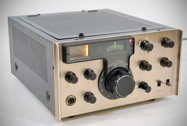
The Kenwood T-599D is an HF transmitter designed to complement the R-599/R-599D series receivers. It uses solid-state circuitry for all low-level signal generation and control functions, combined with a vacuum-tube driver and final power amplifier section.
Features
Hybrid Solid-State & Tube Design: Except for the 12BY7A driver stage and two S2001A final amplifier tubes, the low-level circuits (VFO, carrier oscillator, microphone amplifier, mixers, and VOX) are fully solid-state and modularized on printed circuit boards.
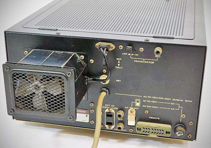
Cooling & Final Protection: Includes a built-in rear cooling fan motor for increased airflow over the shielded final amplifier compartment, ensuring tube longevity under heavy duty cycles.
VFO & Dial Tuning: Utilizes an FET-based VFO circuit utilizing a Clapp configuration and low-impedance Darlington output buffers. The precision tuning drive employs a double gear mechanism covering 100 kHz per dial revolution with 1 kHz resolution.
ALC and Block Bias Keying: Features a transistor-amplified Automatic Level Control (ALC) circuit to prevent splatter and drive distortion. For CW operation, it uses block bias keying with smooth waveform shaping to prevent key clicks.
VOX, Anti-VOX & Semi-Break-In: Equipped with a transistorized VOX circuit with adjustable gain, anti-VOX sensitivity, delay, and a built-in 750 Hz sidetone oscillator for CW monitoring and semi-break-in keying.
AM Operation: Employs low-power amplitude modulation into the IF stage rather than carrier injection over SSB, delivering cleaner AM quality than typical adapted SSB transmitters.
VHF Transvertor Connection: Includes rear-panel transvertor input/output terminals and a toggle switch. When switched to `ON`, screen voltage to the final tubes is disabled and the driver output is directed to an external VHF transvertor (such as 2m or 6m).
Transceive Interfacing: Designed to connect to the R-599D receiver via a 16-pin interconnect cable, enabling unified transceive control, split-frequency operation, or cross-VFO switching controlled from the receiver.
Specifications
Modes of Emission: SSB (A3J), CW (A1), and AM (A3).
Frequency Coverage:
80m (3.50 – 4.00 MHz)
40m (7.00 – 7.30 MHz)
20m (14.00 – 14.35 MHz)
15m (21.00 – 21.45 MHz)
10m (divided into three segments: 28.00–28.50 MHz, 28.50–29.10 MHz, and 29.10–29.70 MHz).
Power Input:
SSB: 200 Watts PEP
CW: 160 Watts DC
AM: 80 Watts DC
Tubes:
(1) 12BY7A (operating in Class A)
(2) S2001A (6146B equivalents, operating in Class AB1).
Semiconductors
4 FETs, 1 IC, 30 transistors, 34 diodes, 3 Zener diodes, and 1 varicap.
– RF Output Impedance: 50 - 75 ohms nominal.
– Audio Input Impedance: Switchable between 600 ohms and 50k ohms.
– Carrier & Unwanted Sideband Suppression: Better than 40 dB down.
Power Requirements: 110–120 V or 220–240 V AC (50/60 Hz), 350 W maximum.