Note
Diameter and Thickness:
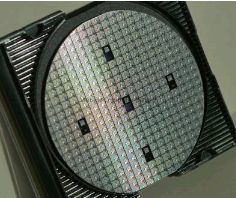
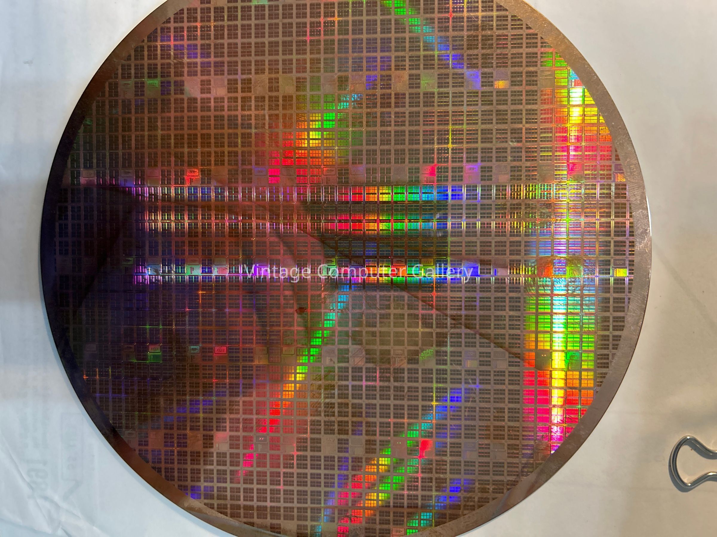
The standard diameter of a 3-inch silicon wafer is 76.2mm (approximately 3 inches). The typical thickness is 380±25µm.
Doping and Resistivity:
Doping refers to intentionally introducing impurities into the silicon crystal lattice to modify its electrical properties.
Common dopants include:
P-type (Boron-doped): Used for creating holes (positive charge carriers). N-type (Phosphorus-doped): Used for creating electrons (negative charge carriers). Resistivity (measured in Ohm-cm) indicates the purity of the silicon. Higher resistivity implies purer silicon but also higher cost.
Crystallographic Orientation:
Silicon wafers are cut from single crystals and have specific crystallographic orientations. The most common orientation is (100), but (110) orientation wafers are used for specific etching processes.
Surface Polishing:
Silicon wafers are typically single-side polished (SSP), but double-side-polished wafers are also available.
Surface roughness is around 1nm (rms basis) due to the chemical-mechanical polishing (CMP) process.
Total Thickness Variation (TTV):
TTV affects the ability to focus on fine details during etching. Standard TTV is <10µm, extra quality is <5µm, and very high precision is <1µm (expensive).
Bow and Warp:
If the wafer is used clamped to a flat reference surface, TTV is relevant. For free-standing use (touching at 3 points), Warp (and its half, Bow) becomes significant. Standard Warp for 3-inch wafers is <30µm.
Crystallization Process:
Most silicon wafers are crystallized using the Czochralski (CZ) process. Dissolved oxygen content is around 20ppma. For processes sensitive to oxygen content, Float Zone (FZ) silicon with <1ppma oxygen is an option (but more expensive).
In summary, 3-inch silicon wafers serve as essential substrates for semiconductor research, microfluidics, and nanoelectrodes. Their properties impact various fabrication processes and applications.